Hi guys!
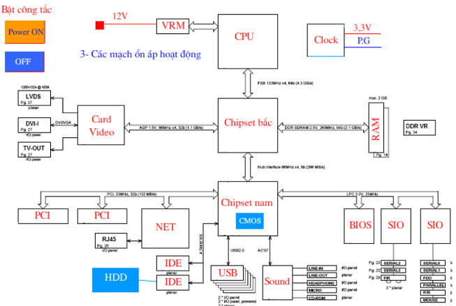
Electronic devices all have different block diagrams, to repair you need to understand the diagram of that device, to know which chip this chip manages, or what task. Makes corrections faster and more accurate. The analysis of the PC manboard block diagram hopes to help you determine the pan faster and more accurately.
On the PC mainboard there are devices such as CPU, RAM, HDD, VGA, DVD drive, network card… These devices have different functions and tasks. So the mainboard plays an intermediary role in connecting the devices into a unified apparatus, the mainboard controls the power supply for the devices, controls the BUS speed (circuit line) for each different device, because the devices These devices run at different bus speeds, the highest being the CPU bus. In addition, the mainboard also generates a clock to activate the components on the mainboard to work. Therefore, if a component dies, the computer will not be able to start, and the process of starting the mainboard will be stopped.

In the picture above is the mainboard block diagram GA-G41MT-S2PT including components: CPU Socket 775, North G41 chipset, PCI e slot, DDR2 slot, ICH7 male chipset, IT8718,bios IO chip…Each component managed by different chips, need to remember clearly to avoid correcting mistakes. Recently, a doctor encountered a mainboard that did not accept the usb, he immediately removed the Northbridge chip instead, while the usb was managed by the male chip, or the machine could not activate the power, he needed to check the 32,768 quartz, check the SIO ic, male chip, then immediately replace the CPU power ic. Those are some cases of not understanding the mainboard block diagram.
* CPU socket: Currently includes common CPU sockets: Socket 775, socket 1155, 1156, 1366, 1150. This socket is controlled by the Northern chipset, the newer mainboards use Intel chips later, the northern chip is integrated. available in CPU for faster speed.
* Chipset North (North bridge): The north bridge chip controls components such as Ram, CPU, video card slot (PCI e slot, AGP slot). These devices have high bus speed, control data back and forth between these components to ensure smooth and continuous. Helps make full use of CPU and RAM speed.
* Chipset South (Sourth bridge): The south bridge chip controls components with a bus speed smaller than the northbridge chip: LAN port, sound, PCI slot, USB port, Bios, SATA hard drive, IDE slot…
* IC SIO (Super In Out): Control the input and output ports of data.
Control PS/2 port, COM port, LPT port. Monitor other components on the motherboard to work to signal that the components are good or to report problems when there is a problem. In addition, it also has a built-in trigger and open source circuit.
* ROM BIOS (Read only memory – Basic in out system): Is a read-only memory IC, the BIOS is loaded by the mainboard manufacturer, the BIOS is usually Ami and Award.
Helps to start the computer and keep the CPU running.
Check for errors of Ram and video card and make a beep in the speaker when there is an error.
Create error messages on the screen such as missing keyboard, mouse, no hard drive, hard drive error… Helps to fix faster.
Manage driver 2 chipset, SIO chip, onboard video card.
The BIOS installer lets you configure which devices to boot, set the date and time, disable lan, sound, or over clock.
In addition, the bios rom also provides a default CMOS installation for the computer to start when we set up the bios or run out of CMOS battery.
* IC Clock Gen : IC generates clock pulses for components on the maiboard to work, if the clocking circuit fails, the computer will not work. This circuit works first when the main has a mains voltage source.
* Voltage stabilizer circuit: The voltage stabilizer circuit on the mainboard helps to provide different power sources, vcore cpu voltage stabilizer circuit, voltage stabilizer circuit for 2 chipsets, AGP slot voltage stabilizer circuit, ram. This circuit outputs voltages like 1.2v, 1.5v, 1.8v, 2.5v, 3.3v. The circuit consists of mosfet lamp components, filter capacitors combined with coils, oscillating ic.
* PCI e and AGP slots: The video card slot leaves the PCI express slot to take the 12v voltage on the mainboard and then onto the card, the pci e card has a voltage regulator circuit located on the card. While the AGP card uses a voltage of 1.5v or 3.3v on the mainboard. This slot is controlled by the northbridge chip.
* Ram slot: Used to attach Ram DDR, DDR2, DDR3… Depending on the type of ram that has different bus speeds, ddr2 ram cannot be mounted on ddr3 slot and vice versa. The ram slot is also controlled by the northern chipset.
* PCI slot: This slot is controlled by the male chip, used to attach expansion cards: lan card, sound card, usb card, wifi card.
* SATA port, IDE port: These ports are controlled by the male chip used to attach CD and HDD devices.
* USB port, panel port: Because the male control chip is used to connect usb devices, the panel port is used to connect to the front of the case for usb and audio.
Hope you have to remember the mainboard block diagram. This is the most important knowledge in computer hardware repair.


